|
|
|
|
Probe
Card Basics
|
|
|
|
This section is intended to provide general information about
the function of a probe card, as well as an introduction to
its primary components. This is not to provide any specific
manufacturing instructions, but simply to help answer the question,
“What is a probe card?”
The type of probe card introduced here is generally known as
an epoxy-type probe card. The technology is relatively simple
and in contrast to the rapid advances being made in IC device
technology each year, the epoxy-type probe card has remained
relatively unchanged. With smaller device sizes and increasingly
tight requirements, however, industry is beginning to demand
an advance in probe card technology as well. New materials and
manufacturing methods are slowly being introduced. In spite
of these changes, the epoxy-type probe card has remained an
integral part of the IC testing process.
|
|
General Function
1.1 The Integrated Circuit
Semiconductor Integrated Circuits (ICs) are essential in
today’s high-tech society. They can be found at the
heart of a variety of products, from the simplest calculators
to the fastest computers. As a result, the production of ICs
has become a billion dollar industry, involving some of the
world’s most advanced technology. Probe cards are important
in the final phase of this production process, playing a vital
role in the testing and measuring of integrated circuits.
Integrated circuits are built from round, thin sheets of
semiconducting material. Standard sheets, or wafers, are commonly
made of silicon. These wafers can range from 5 cm (~2 in)
to 20 cm (~8 in) in diameter and are roughly 0.10 cm (~0.04
inch) thick. On a single wafer, anywhere from 50 to 200 identical
integrated circuits, or die, can be made. The process of taking
a simple silicon wafer and creating from it circuitry which
can use and store electricity is a complex process. In a sense,
the circuitry is “embedded” in the silicon, just
below its surface. Within this microscopic maze of circuitry,
electrical signals flow from one point to the next, much in
the same way that water flows in a riverbed. To interact with
the world outside of the IC, these signals are passed back
and forth through small metal pads attached to the wafer’s
surface (see Figure 1-1). The ability to make electrical contact
with these metal pads is critical. Without some method of
making this contact, the integrated circuit can not be used. |
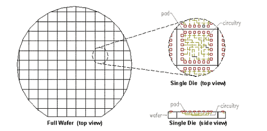
Figure 1-1: Integrated Circuit Wafer |
1.2 Testing the IC
In the testing of integrated circuits, probe cards play this
vital role of contacting the metal pads on a wafer’s
surface. ICs are tested by large machines, called testers,
which send a series of electrical signals to each IC. During
testing, the probe card and IC are held in place by another
machine, called a prober. The prober might be described as
the "arm" of a tester, doing the mechanical work
of moving and aligning the probe card and IC. The probe card
then functions primarily as the "hand" of a tester,
allowing it to "touch" the metal pads on a wafer’s
surface (see Figure 1-2). This establishes an electrical connection
between tester and IC, allowing signals to flow freely between
them. An ICs response to these test signals then indicates
whether it has been made correctly. Good ICs can then be separated
from bad ones. Probe cards are at the center of this testing
process.
|
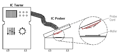
Figure 1-2: IC Tester and Prober (with probe card and wafer)
|
With the help of the prober, the probe card is lowered onto
the IC wafer until the probe tips come into contact with the
wafer’s metal pads. Test signals can then be passed
between tester and IC.
|
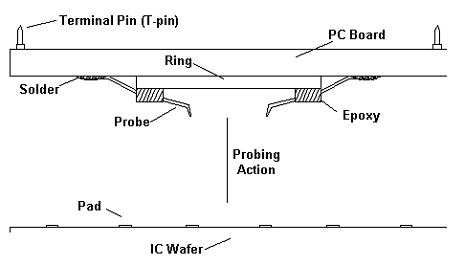
Figure 1-3: Probe Card and Wafer |
The movement of the probes as they touch the surface of the
metal pads is also important. Generally, the surface of each
metal pad is covered by a very thin layer of glass-like material,
called an oxide. In order to make contact with the metal underneath,
the probe tips must break through this thin oxide.
Because the probes are very thin, roughly 0.250 mm (~0.010
in) in diameter, they flex when touching the wafer. As they
flex, the probe tips slide, or scrub, across the surface of
the pads (See Figure 1-4). This scrubbing action causes the
probe tips to break through the surface oxide, helping make
good electrical contact with the metal underneath.
|
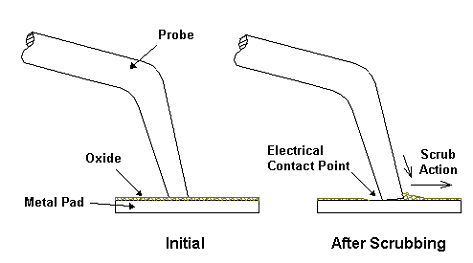
Figure 1-4: Probe Scrub Action
|
Although its basic function is relatively
simple, building a probe card requires precise and careful
work. Probe cards are an assembly of a variety of parts, some
fragile and some sturdy. In the following chapters, you will
be introduced to the primary components which make up a standard
probe card. Because no two probe cards are exactly the same,
each component is described in its most common form. |
Probe
2.1 Function
Earlier in section 1.0, a probe card was described as the
“hand” of the tester. If we think of a probe card
in this way, the probes then function as its "fingers."
As was shown in Figure 1-4, the probe is the part of a probe
card that actually makes contact with the integrated circuit.
2.2 Straight Probes |
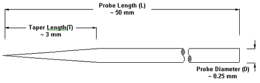
Figure 2-1: Straight Probe (not to scale) |
|
Generally, if probes are purchased from a vendor, they arrive
just as shown above in Figure 2-1. They are straight, thin,
needle-like pieces of metal, with one end that tapers down
into a sharp point. Probes are most commonly made of Tungsten
(W) and Rhenium Tungsten (ReW), although materials such as Beryllium Copper (BeCu)
and Palladium (Pd) are also used. A straight probe is defined by four
basic parameters: material, probe length (L), probe diameter
(D), and taper length (T). Common material and dimensions
are listed below in Table 2-1.
|
Table 2-1: Straight Probe parameters
|
| 2.3 Bent Probes |
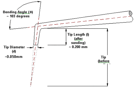
Figure 2-2: Bent Probe
|
Before a probe card is assembled, the tapered
end, or tip, of these straight probes must be bent. Again,
depending on a customer’s specifications, these tips
can be bent at a variety of angles, although 103 degrees is
standard. Throughout the assembly process, the shape of a
probe remains just as it has been bent, with a sharp, pointed
tip. After a probe card has been fully assembled, however,
these probe tips are sanded down to create a desired tip diameter
(d) and tip length (l). Including the parameters from Table
3-1, a bent probe is defined by seven parameters, which are
listed below in Table 2-2.
|
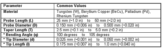
Table 2-2: Bent Probe parameters
|
Ring
3.1 Function
|
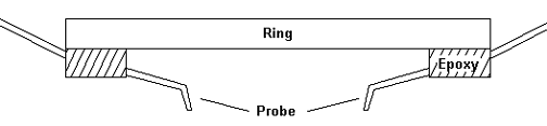
Figure 3-1: Assembled Ring
|
| A probe card ring’s basic
function is straight forward. It is simply a sturdy piece of
material to which the probes are attached. Once the probes are
attached to the ring, they can conveniently be handled and operated
as a single unit. |
3.2 Material
Although a ring’s basic function is purely mechanical,
the type of material it is made from is very important. A
ring must be
- sturdy, to give the probes a firm foundation,
- electrically non-conductive, to protect the test signals
being passed through each probe,
- able to withstand high temperatures, sometimes as high
as 200 deg C (~392 deg F).
To meet all of these requirements, ceramic is often used.
|
3.3 Shape
The size and shape of a ring depends on the IC device which
will eventually be tested. It is most common for the pads
to be arranged along the outer edge of an IC device. When
probing a single die, this results in a ring that is most
often square or rectangular, as shown in Figure 3-2.
|
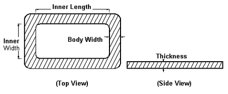
Figure 3-2: Standard Rectangular Ring
|
Rings, too, come in all shapes and sizes.
A few examples are shown below in Figure 3-3.
|
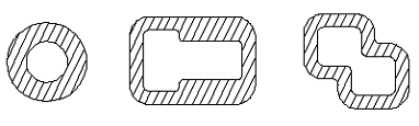
Figure 3-3: Ring Examples |
3.4 Epoxy
In order to attach the probes to the ring, a special glue,
or epoxy, is used (see Figure 3-1). Although the ring provides
support for the probes, it is the epoxy which actually holds
the probes in place. After curing, an epoxy generally has
properties similar to those of the ring. It must be very sturdy,
electrically non-conductive, and be able to withstand high
temperatures. In addition, an epoxy must adhere itself well
to both the ring and the probes, in order to hold the probes
in position.
A variety of epoxies are used in the probe card industry.
Some are designed for high temperature applications, while
others are designed for low leakage applications. The epoxy
which is used for any individual probe card depends primarily
on the customer’s requirements.
|
Printed Circuit Board
4.1 Function
The largest of the components which make up a probe card
is the board. It functions both as a support for the assembled
ring, as well as the point where test signals are passed from
the probes to the prober. Because the test signals pass through
the board, it is also a convenient place to mount components,
such as capacitors, resistors, and relays. These components
can then help in manipulating and controlling the test signals
as they are passed back and forth between tester and IC.
|
4.2 Material and Shape
A few different materials are used in making a board, the
choice of which depends on a customer’s testing temperature
and leakage requirements. As was true of both the ring and
epoxy, the main board material must also be electrically non-conductive.
A type of fiberglass, FR-4, is commonly used, as well as polyimide.
To carry the test signals, thin strips of metal run along
the top and bottom of the board.
Unlike the ring and probes, which are designed entirely to
match the IC, the board is designed to match the prober. For
this reason, boards come in many sizes. Although there are
many sizes, they come in two basic shapes: round and rectangular.
Round boards commonly range in diameter from 5.7 cm (~2.25
in) to 34 cm (~13.5 in), while rectangular boards are roughly
11.5 cm (~4.5 in) X 21.5 cm (~8.5 in).
|
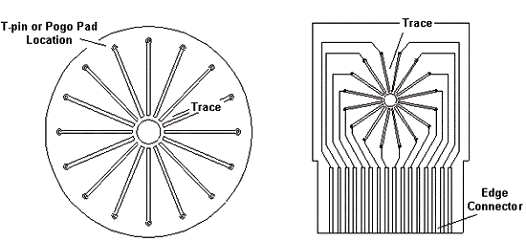
Figure 4-1: Common Boards (bottom side view)
|
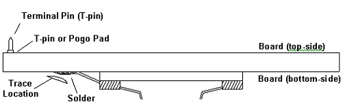
Figure 4-2: Round Board, Trace and T-Pin Location
|
4.3 Traces
The thin strips of metal located on the bottom-side (or ring-side)
of a board are called traces (see Figure 4-1). It is here
that the probes are soldered to the board (see Figure 4-2).
These traces are very much the same on most boards, regardless
of size or shape.
|
4.4 T-pin, Pogo Pad, and Edge Connector
As was mentioned in section 4-1, the board must also connect
to the prober. While the probes are generally soldered to
the traces near a board’s center, the prober connection
is usually made near a board’s outer edge. The way this
connection is made depends on the type of prober, but there
are generally three methods which are used. They are as follows:
|
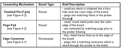
Table 4-1: The Board/Prober Connection
|
Key Parameters
Here is a general diagram of a completed probe card, labeled
with a few of the more important parameters. See the following
table for additional explanation.
|
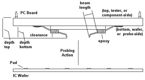
Figure 5-1: Probe Card and Wafer
|
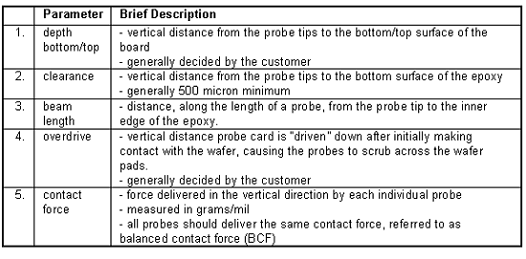
Table 5-1: Key Parameters |
 |
|
|
|
|
|
|
|